‘No way back is the way to victory:’ Huawei senior executive on ‘Tau Scaling Law’ R&D process
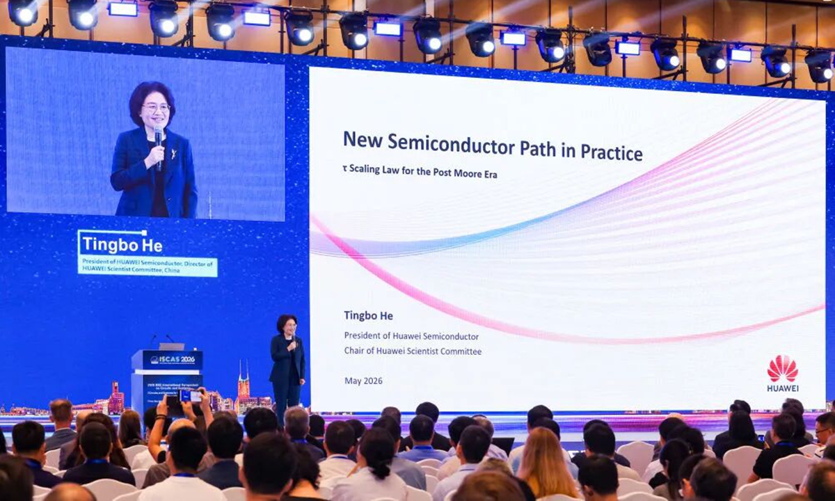
He Tingbo, president of Huawei's semiconductor business department Photo: Screenshot of Xinhua News Agency's report
He Tingbo, president of Huawei's semiconductor business department, in an interview with the Xinhua News Agency following the company's unveiling of the "Tau Scaling Law," revealed the milestone research journey behind the breakthrough and the hardships endured along the way, stating that "No way back is the way to victory."
Huawei unveiled what it calls the " Tau Scaling Law" on Monday — the first time a Chinese high-tech company has put forward a new guiding principle for the global semiconductor industry. Under the principle, it expects Huawei's advanced chips to achieve transistor density equivalent to a 1.4-nanometer process node by 2031, He said.
As the Moore's Law has guided the semiconductor industry for more than 50 years, driving performance gains and cost reductions through the continuous shrinking of transistor sizes. But as transistors approach physical limits and chip research and development costs have surged, that path of semiconductor evolution has become increasingly unsustainable, said the Xinhua report.
The "Tau Scailing Law", named after the Greek letter tau (τ), offers a different answer, He Tingbo explained: the industry must look not only at space, but also at time — examining at every level, from transistors and circuits to chips and data centers, to make sure that transmission latency, synchronization, and computation time can be reduced, consistently.
He Tingbo likened the concept to transforming a "flat city" into a "three-dimensional city," with millions of elevators installed between urban districts. Logic folding, she said, is not simply about stacking layers, but about restructuring information pathways so the entire system could complete tasks faster.
The executive's remarks also touched on Huawei's years of struggle in the past seven years. After Washington moved to restrict the company in May 2019, she issued an internal letter announcing that Huawei's chip "backup plan" was being totally activated — a move that drew widespread attention at the time. Reflecting on the hardships since, she said: "No retreat, sometimes, means the only way is the path to victory."
Huawei also formed a research group codenamed "Moye" — named after an ancient Chinese legend in which a swordsmith achieves the forging of a pair of legendary blades "Ganjiang" and "Moye" through fearless sacrifice. Though called a "group", its ranks have swelled to tens of thousands. He said the name captures the spirit of those who endured years of hardship to contribute to the company's incessant tech breakthroughs.
Guided by the "Tau Scaling Law," Huawei has developed 381 chips over the past six years used for telecommunications, smartphones, general computing, and AI computing. This autumn, the company plans to release a new high-end Kirin chip — the first to fully implement the logic folding technology, according to He Tingbo.
The "Tau Scaling Law" represents a breakthrough in Huawei's fundamental tech research, He Tingbo said, with significance extending beyond chips to the semiconductor industry as a whole. "No single company can have all the answers in the next decade. We welcome like-minded partners from academia and industry to join us in tackling the common challenges facing the electronics sector and exploring a path forward together," she said.
Global Times
RELATED ARTICLES