China’s major scientific facility High Energy Photon Source opens first global call for user research proposals
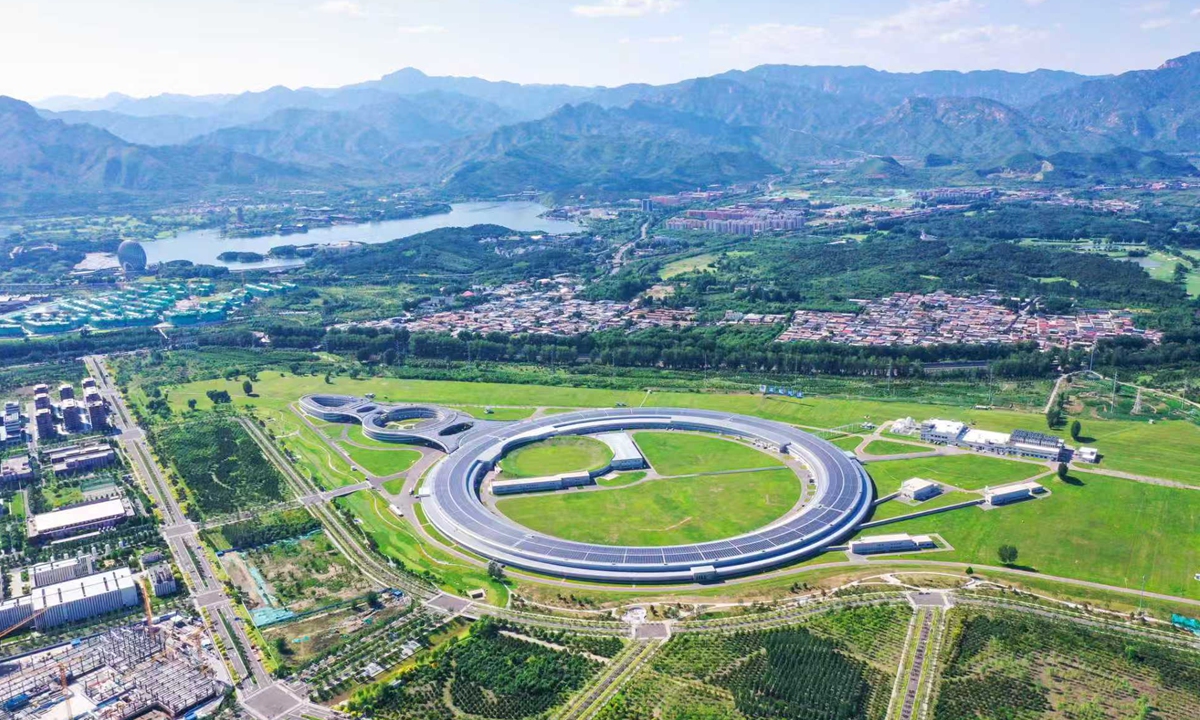
Aerial view of the building of High Energy Photon Source. Photo: Courtesy of the Institute of High Energy Physics, Chinese Academy of Sciences
China's High Energy Photon Source (HEPS), a major national scientific facility often dubbed a "super microscope" and giant "X-ray machine," has recently opened its first global call for user research proposals. The move signals the project's shift from construction to preparations for full operation and marks a key milestone in the country's fourth-generation synchrotron radiation program, the Global Times learned from the Institute of High Energy Physics, Chinese Academy of Sciences, on Tuesday.
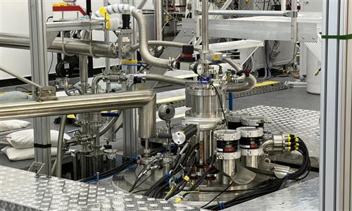
Located at Huairou science city, HEPS is China's first high-energy synchrotron radiation facility. It is also Asia's first and the world's fifth fourth-generation synchrotron light source facility with the highest designed brightness in the world. Comprising an accelerator and beamline stations, the facility operates on the basic principle of accelerating electrons to generate light, providing users with customized, high-quality X-rays for scientific experiments.
According to the institute, HEPS is capable of accommodating at least 90 beamline stations. In its first phase, 14 user beamlines and one test beamline have been constructed.
The facility can provide X-rays with energies of up to 300 kiloelectron volts and offers nanometer-scale spatial resolution, picosecond-scale time resolution, and energy resolution at the millielectron-volt level.
These capabilities will help researchers better "observe" the microscopic world and characterize the microstructures of materials, as well as reveal the processes and evolution mechanisms.
After more than six years of development and construction, HEPS began trial operations and started user experiments on December 3, 2025. By mid-February 2026, the facility had supported 222 experiments for 91 institutions, providing nearly 5,000 hours of beam time to users from universities, research institutes, and leading enterprises from China and abroad.
In areas such as defect detection in aerospace material, ultra-fast imaging during the 3D printing process of materials, mesoscopic neural connectivity mapping of monkey brain, in-operando measurement in battery device and 3D nano imaging of semiconductor nanostructures, pilot user experiments with the HEPS have achieved better-than-expected results or successfully completed validation tests. These results have laid a solid foundation for more in-depth research in the future.
To prepare for its official operation, the HEPS has opened its first global call for research proposals for all the user beamlines in phase I, with applications accepted until April 30, 2026, and approved projects remaining valid for two years, according to the institute.
The HEPS team will work closely with user institutions worldwide to support research and development across key sectors such as aerospace, biomedicine, new-energy batteries, semiconductors, petrochemicals, energy and environmental technologies, and nanomaterials, with the aim of accelerating industrial upgrading.
RELATED ARTICLES